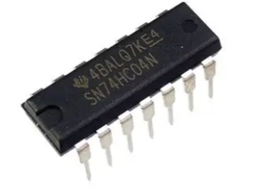
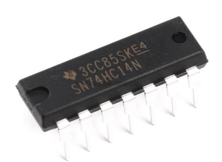
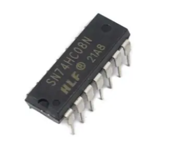
74HC04 Hex Inverter Logic Gate IC
= High-Speed CMOS Hex Inverter for Digital Logic and Signal Inversion =
The 74HC04 is a high-speed CMOS logic IC containing six independent inverting buffers. Each inverter produces a HIGH output when the input is LOW, and a LOW output when the input is HIGH. This basic yet essential logic function is used for signal inversion, level shifting, oscillator circuits, and interface conditioning in digital systems.
Operating voltage range: 2.0V to 6.0V
Propagation delay: 7ns typical at 5V
Output drive capability: ±5.2mA at 6V
Do not exceed 7.0V supply voltage - permanent damage may occur
Unused inputs must be tied to VCC or GND - floating inputs can cause oscillation
= Technical Specifications =
| Parameter | Value |
|---|
| Supply Voltage (VCC) | 2.0V to 6.0V |
| Input Voltage | 0V to VCC |
| Output Current (High/Low) | ±5.2mA (at 6V) |
| Propagation Delay | 7ns typical at 5V |
| Quiescent Current | 2µA typical (at 6V) |
| Operating Temperature | -40°C to +125°C |
| Package Types | DIP14, SOIC14, TSSOP-14 |
| Number of Inverters | 6 (hex buffer) |
= Pin Configuration (DIP14/SOIC14/TSSOP-14) =
| Pin | Name | Function |
|---|
| 1 | 1A | Inverter 1 Input |
| 2 | 1Y | Inverter 1 Output |
| 3 | 2A | Inverter 2 Input |
| 4 | 2Y | Inverter 2 Output |
| 5 | 3A | Inverter 3 Input |
| 6 | 3Y | Inverter 3 Output |
| 7 | GND | Ground (0V) |
| 8 | 4Y | Inverter 4 Output |
| 9 | 4A | Inverter 4 Input |
| 10 | 5Y | Inverter 5 Output |
| 11 | 5A | Inverter 5 Input |
| 12 | 6Y | Inverter 6 Output |
| 13 | 6A | Inverter 6 Input |
| 14 | VCC | Supply Voltage (2V to 6V) |
= Truth Table (Per Inverter) =
| Input | Output |
|---|
| LOW | HIGH |
| HIGH | LOW |
Inverter simply complements the input signal - HIGH input gives LOW output and vice versa
= Key Features =
Six Independent Inverters Multiple inverters in a single 14pin package
Wide Supply Range - Operates from 2V to 6V for flexible system integration
Low Power Consumption 2µA quiescent current ideal for battery-powered designs
High Noise Immunity - VIH/VIL specifications ensure reliable operation
Compatible Inputs - Accepts both CMOS and TTL drive levels
Schmitt Trigger Action - Clean switching even with slow input edges
== Applications ==
- Signal inversion and level shifting
- Crystal and RC oscillators
- Pulse shaping and edge detection
- Clock signal buffering and conditioning
- Logic level translation
- Waveform generation
- Interface conditioning between different logic families
- Industrial control logic
- LED driver circuits
- TTL/CMOS interface logic
Six Inverters in One Package - Maximizes board space utilization
Fast Propagation Delay 7ns typical for highspeed applications
√ Industry-standard 74HC04 pinout for easy replacement
√ Low power consumption - 2µA typical quiescent current
√ Fully tested and guaranteed functional
= Package Includes =
| 1. *1x* 74HC04 Logic IC (Package | DIP14, SOIC14, or TSSOP-14 per variant) |
- Anti-static packaging for safe delivery
For crystal oscillator circuits, use one inverter with feedback resistor and two capacitors
Use inverter as buffer by cascading two inverters in series
This IC is also available as 74HCT04 for TTL-compatible input levels
Inverter with input tied LOW produces constant HIGH output
Inverter with input tied HIGH produces constant LOW output
Multiple inverters can be used to create ring oscillators for clock generation
For LED driving, use inverter to sink current from LED to ground
Never leave inputs floating use pullup or pull-down resistors
ESD sensitive device - use proper handling procedures
Ensure decoupling capacitor (0.1µF) is placed near VCC pin